
5
Molecular workstations
Five independent systems are running experiments in parallel; a single workstation going down never halts scientific progress.
CBN Nano designs our own proprietary technologies, incorporating them into our instruments and enabling atomically precise fabrication. We run our own quantum chemistry simulations and then build and verify structures one reaction at a time.
CBN Nano combines purpose-built molecular tools, cryogenic scanning probe microscopes, atomistic simulation, automation, and direct verification in one integrated operating platform.
Five independent systems are running experiments in parallel; a single workstation going down never halts scientific progress.
Logged additive and subtractive operations across carbon, hydrogen, iodine, and silicon.(Updated Monthly)
Additive donation and subtractive abstraction demonstrated across hydrogen, silicon, and carbon-based operations.
Ultra-high-vacuum workflows designed for controlled reactions and atomic-scale imaging.
Fabricated structures are characterized at each step, confirming the performed operation yields the intended product.
Tool design and synthesis are integrated with experimental requirements and platform development.
Most groups working at the atomic scale rent, borrow, or outsource the hardest parts of the problem. CBN Nano owns them. We engineer our own instruments, synthesize our own molecular tools, and run our own simulations — an integration that lets us move from idea to verified structure without waiting on anyone else.
Our engineering team designs, builds, and continuously improves custom ultra-high-vacuum and cryogenic systems, inverted-mode STM, and the Silicon Probe Chip platform — while keeping every workstation productive. With five independent molecular workstations, a single system going offline for maintenance or an upgrade never stops the science.
Deterministic atom placement requires finely-tuned molecular tools. We design and synthesize purpose-built, functionalized molecular tools tailored for the desired application.
Atomistic simulation designs candidate reactions ahead of the experiment and validates what the STM measures afterward — closing the loop between what we intend to build and what we prove we built.
Chemistry, engineering, simulation, fabrication, and verification are not partners we coordinate — they are teams that sit together. That integration is the platform.
Five independent molecular workstations pair ultra-high-vacuum chambers, cryogenic scanning probe microscopy, and in situ characterization to build and verify structures at the level of chemical bonds — operating in parallel in Ottawa today, so the work never depends on a single system. The lab is housed within a high-security Canadian Bank Note Company, Limited facility, protecting both the instruments and our partners' intellectual property.
A closer look inside our Ottawa facility: the cryogenic ultra-high-vacuum molecular workstations and support infrastructure, where atomistic structures are fabricated and verified, one chemical reaction at a time.
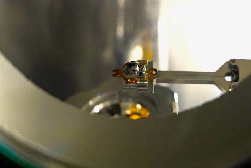
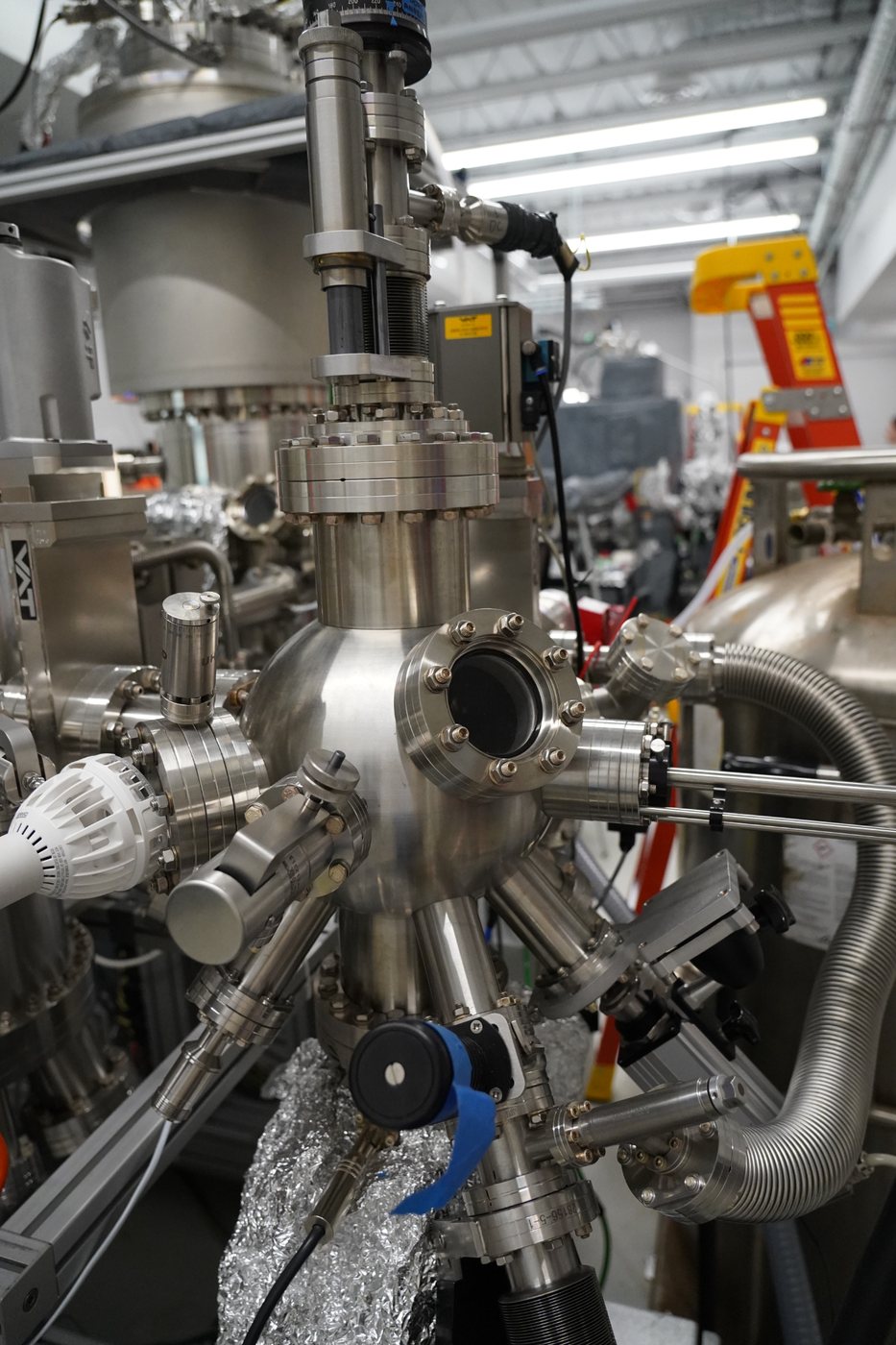
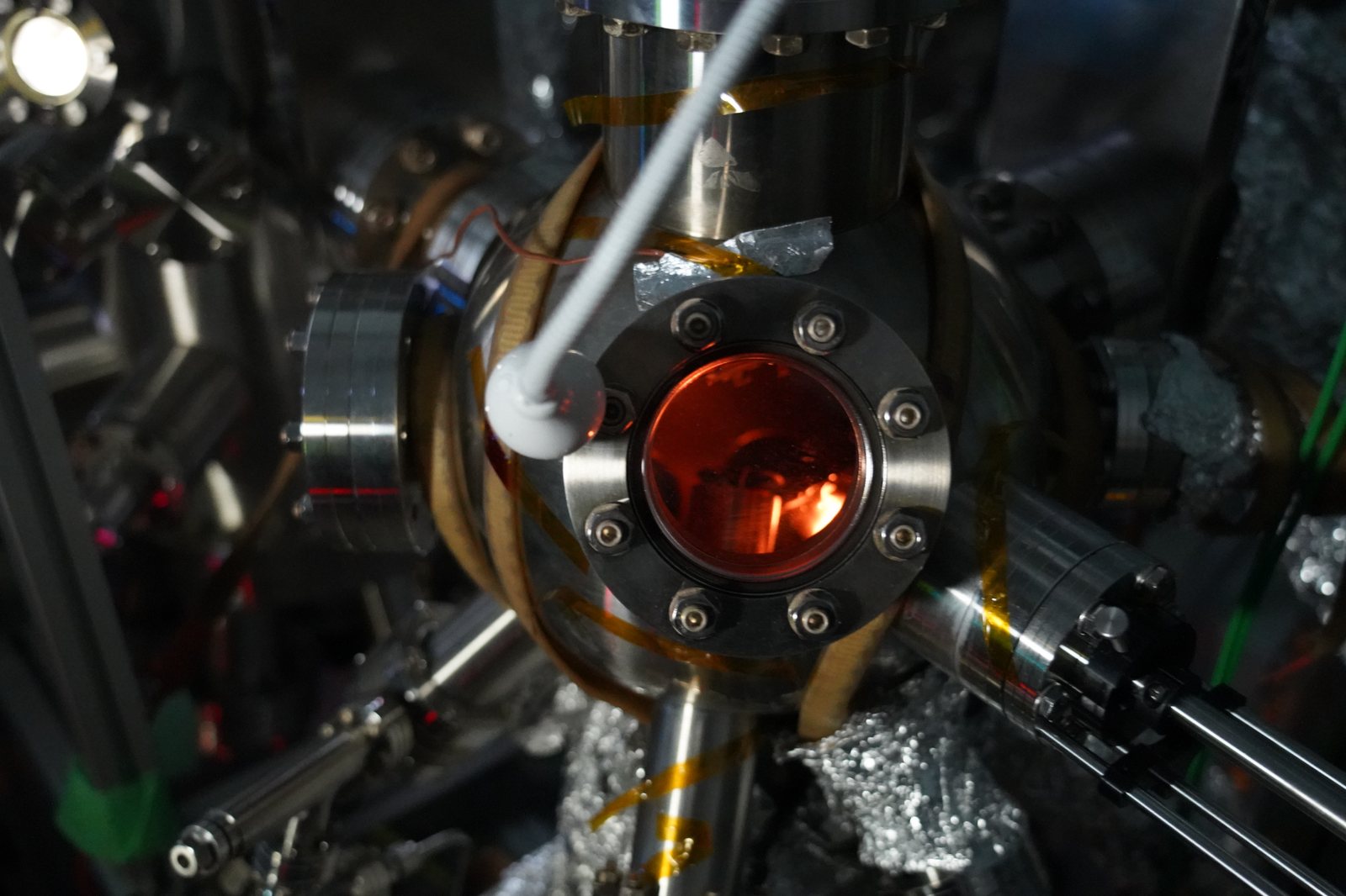
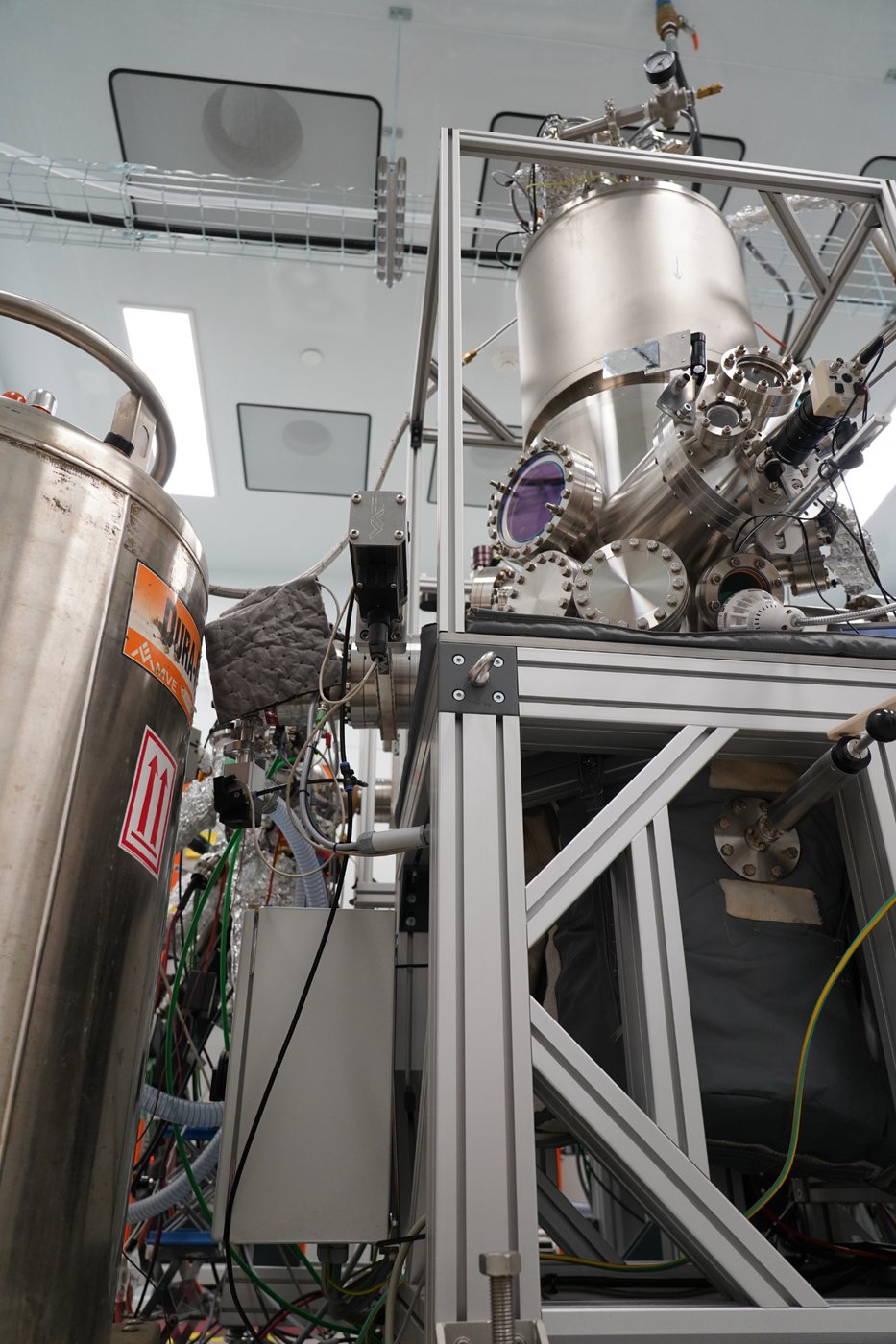
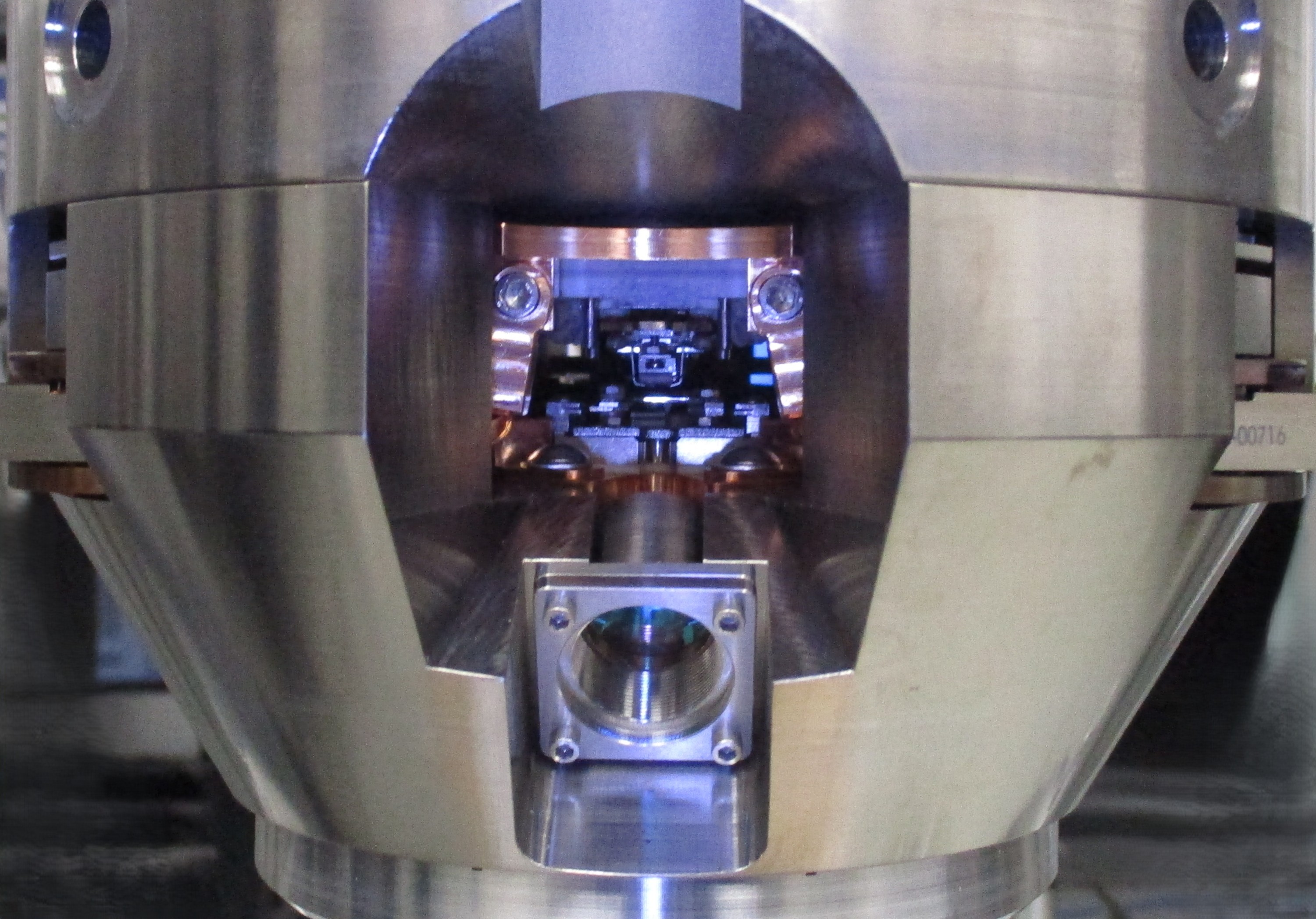
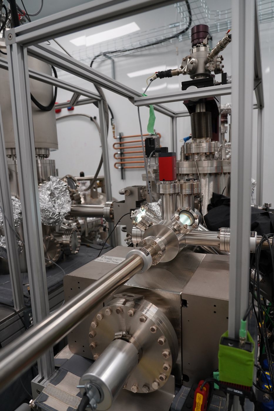
Photographed in CBN Nano's Ottawa laboratory. Every image is real equipment in active use — part of five independent molecular workstations running in parallel.
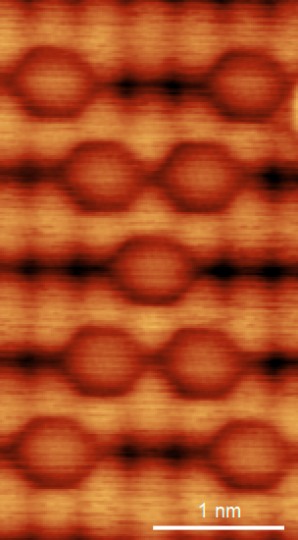
The image beside this text is a direct scanning tunneling micrograph from our lab — individual carbon atoms resolved on a silicon surface, imaged at the atomic scale.
Where others model atomic precision, CBN Nano demonstrates it: we build the structure, then we verify it, closing the loop between design and physical reality.
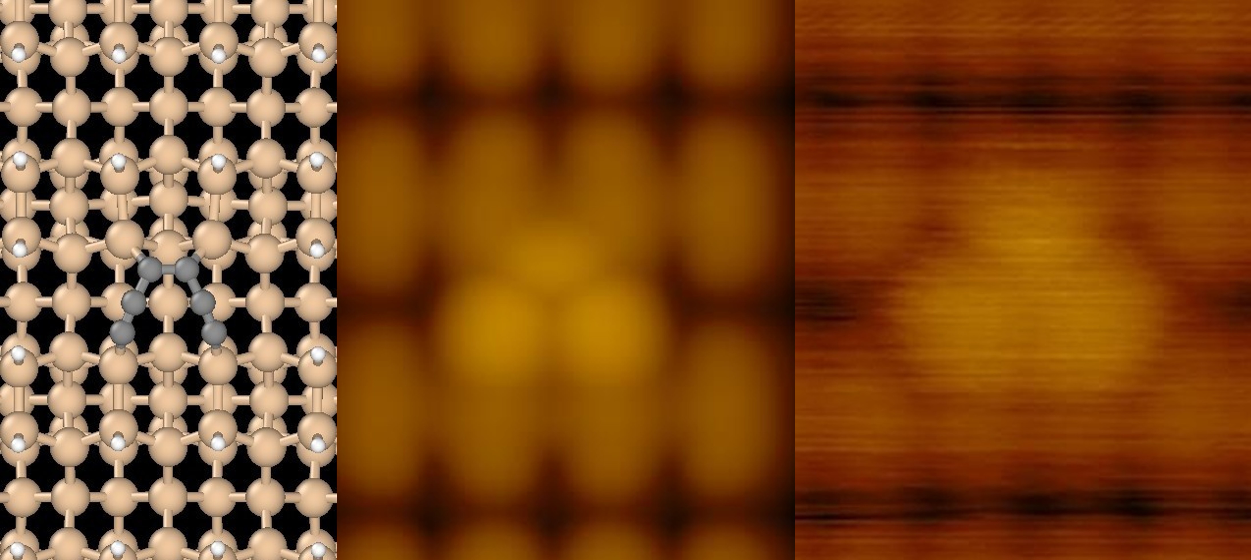
On the left, a ball-and-stick model of the target structure. In the center, simulated STM image based on the model. On the right a real scanning tunneling micrograph of a six-carbon structure with a footprint spanning two inter-rows on Si(100). We've built this structure by three successive C₂ dimer transfers.
Our platform doesn't just place atoms — it patterns them. This is a real scanning tunneling micrograph of a 3 × 3 array of inter-row C₂H units, each one mechanosynthetically placed and covalently bonded to the Si(100)-2×1 surface. Every dimer is a designed placement, not an accident of chemistry — nine deliberate pairs of bonds in a regular grid. Repeat that control across a surface and you have programmable matter.
Every dimer is a designed placement, not an accident of chemistry — nine deliberate pairs of bonds in a regular grid. Repeat that control across a surface and you have programmable matter.
9 × C₂H units · deterministic placementCBN Nano's evidence base spans complementary donation and abstraction operations, bond formation, patterned structures, and direct experimental verification.
Controlled transfer of C₂ units to prepared reactive sites.
Successive fabrication steps used to extend designed carbon structures.
Subtractive removal of selected silicon atoms using molecular tools.
Controlled placement of silicon atoms onto defined atomic sites as an additive fabrication operation.
Targeted removal of hydrogen from passivated silicon sites.
Controlled transfer of hydrogen to selected atomic sites, enabling complementary additive hydrogen operations.
Multiple carbon dimers placed in selected arrangements on silicon.
Measured STM structures compared against atomistic simulations.
Fabrication results assessed directly before subsequent operations.
Sequential operations used to move beyond isolated atomic events.
The roadmap focuses on expanding capability, repeatability, automation, throughput, and application relevance.
Future capabilities represent development direction and are not commitments to specific delivery dates.
We are opening pilot programs with quantum companies and research partners. If atomic precision is on your roadmap, we should talk.
Discuss a Feasibility Study